Posts

Showing posts from August, 2019

LED

Image
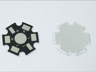
We are professional LED PCB manufacturer . We offer all kinds of LED PCB Product  and our LED PCB price  is competitive.  For High-Power LED of the Aluminum Base PCB, copper base PCB, ceramic base PCB, for low-power LED of the FR4 PCB, High-Temperature PCB. As the Aluminum Base PCB of good thermal performance, High-Power LED products most commonly used Aluminum Base PCB.   We can give different Solder mask options for your Led PCB ,We do lots of R&D on Led PCB solder mask  Lumens to give your Led lights better brightness . The Applications of LED PCB Circuit Board The Led benefits  make LED printed circuit boards  very desirable for a number of applications and industries. Some of the more prominent applications of Aluminum LED PCB Circuit Board include:Telecom LED PCB,Automotive LED PCB,Computer Led PCB,Medical LED PCB,Led PCB Products :  Led Tube , Outdoor LED advertising screen, LED Lamp, Waterproof Led , 1.5m Led and so on .   Led PCB Materials We support: ·  Fr4 PCB R

Education

Image
Students are our future engineers who will re-shape the world surrounding us. Some of the most creative and audacious electronic research comes from our students in universities or even high schools.   PCB education  is important nowadays.  Therefore PCBSky.com feels proud to sponsor teachers and students for their PCB needs. The biggest challenge of modern electronics is that the components are so miniaturized that students can no longer use universal boards and the parts can no longer be reliably hand soldered. By streamlining manufacturing processes, PCBSky.com is capable to fabricate your PCBs in as short as 12 hours, and offers PCB assembly under one roof as a consecutive service. Our strong network of parts suppliers makes the sourcing quick, reliable and cost-effective.

What is pcb used for?

With the development of science and technology, the application of PCB is more and more extensive. PCB is divided into single-sided PCB, double-sided PCB and multi-layer PCB. Common multi-layer boards are generally 4-layer PCB or 6-layer PCB, complex multi-layer board. It can be used in dozens of layers and is widely used in consumer electronics, computers, communication tools, medical equipment and other fields. In terms of application industry distribution, consumer electronics accounted for the highest proportion, up to 39%; followed by computer accounted for 22%; communication accounted for 14%; industrial control, medical instruments accounted for 14%; automotive electronics accounted for 6%; Aerospace accounts for 5% of the total, and the requirements for PCB precision in aerospace and medical instruments are very high. Although China's current PCB industry scale is the world's first, but from the overall technical level, it still lags behind the world's advanced leve

Computers&SSD

Image
The PCB on the computer consists of a motherboard, a hard disk, a memory module, a graphics card, and the like. The plane of the computer motherboard is a PCB (printed circuit board), generally four or six layers. Relatively speaking, in order to save costs, the low-end motherboards are mostly four-layer boards: the main signal layer, the ground layer, the power layer, and the sub-signal layer, while the six-layer board adds the auxiliary power layer and the middle signal layer. Therefore, the six-layer PCB The motherboard is more resistant to electromagnetic interference and the motherboard is more stable. You won't find electronics PCBs today only in computers - although laptops, smartphones, desktops and tablets certainly can't function without quality printed circuit boards, and printed circuit boards for computers make up a large part of the industry. Instead, you'll find machines containing printed circuit boards almost everywhere you look. Your television, wireless

Warmly celebrate our company's national high-tech enterprise certification

Image
After more than a year of hard work, our company finally passed the national high-tech enterprise certification.

What are the Factors that Affect the Price of PCB Processing

PCB processing belongs to the OEM customer's OEM products. Different customers order different products, and there are few shared products. On the other hand, some customers may specify the use of a manufacturer's substrate for quality considerations. Ink and so on, in order to achieve its quality and cost control requirements, so PCB processing prices are changeable. What are the factors that affect the price of PCB processing? Basically consists of the following factors: First, the materials used in the PCB are different. Taking ordinary double-panel as an example, the sheets generally have FR-4, CEM-3, etc., the thickness ranges from 0.6mm to 3.0mm, and the thickness of copper varies from 1oz to 3oz. The price varies greatly from specification to specification; In terms of ink, there is also a price difference between ordinary thermosetting ink and photosensitive green ink, so the difference in materials causes price diversity. Second, the PCB uses different production proc

Role of auxiliary components in hard gold plating PCB plating solution

Image
Electroplating can be divided into hard gold and soft gold. Hard gold electroplating is an alloy, so its hardness is relatively hard. It is suitable for use in places requiring force and friction. It is generally used as the edge contact point of PCB (commonly known as golden finger). Soft gold, On the other hand, is commonly used to connect aluminum wires On the COB (Chip On Board) or On the touch surface of mobile phone keys, and more recently, it is widely used On both sides of BGA boards. The distinction of hard gold and soft gold, it is the component of this layer of gold that goes up finally plating, when gold-plating can choose electroplate pure gold or alloy, because the hardness of pure gold is softer, so also call "soft gold". Function of auxiliary components in   hard gold plating PCB   plating solution: Boric acid ACTS: as a buffer, which can maintain a relatively balanced PH value of hard gold-plated PCB plating solution with a concentration of 35~55g/l; N

What Information does the PCB Prototype Need to Give the Manufacturer

Recently, many customers asked the PCB Prototype what information to provide, and today I will give you a comprehensive answer. PCB Prototype is an early step in mass production. Only when proofing is accurate, can it be put into mass production. Therefore, it is especially important to provide accurate proofing files. So, do you know what documents you need to provide? And what issues should I pay attention to in the documentation provided? First, you need to provide a PCB or GERBER file, the document should include the plate-making instructions - including the specific number of board layers, materials, pad process, ink color, etc., here are some specific parameters to explain. Material: To explain what kind of PCB material is needed, the most common one is FR4. The main material is epoxy resin stripping fiber board. Slab: Describe the number of layers in the PCB. (The PCB production layer is different, the price will be different, and the PCB Prototype process is much the same) Sold

This PCB Manufacturer is Different

We often hear that PCBs are everywhere in the Shenzhen area of China. In our eyes, the PCB factory is a particularly cheap factory, but this board manufacturer is different. What is the truth? This board processing plant has a strict quality control system: 1 product meets IPC-II or IPC-III standards 2 use SPC management chart for quality process control 3 Implement PDCA cycle process to continuously improve product performance 4 Established a complete quality assurance inspection system, the entire process is equipped with professional quality assurance personnel In the circuit board industry, there are often customer complaints that the delivery time is not on time, and the pcb is not good. Is this the circuit board factory supplier has no choice? Or is the operator not worried? PCBSKY has rich experience in PCB production. As a PCB manufacturer, we have excellent process R&D team, stable production team, strict quality assurance team, excellent quality, accurate delivery and goo

10 PCB Puzzle Secrets

1. The outer frame (clamping edge) of the  custom pcb fabrication  should adopt a closed-loop design to ensure that the PCB panel will not be deformed after being fixed on the fixture. 2. The width of the custom pcb fabrication is less than or equal to 260mm (SIEMENS line) or less than or equal to 300mm (FUJI line); if automatic dispensing is required, the product of the width and length of the PCB board is less than or equal to 125 mm × 180 mm. 3. Custom pcb fabrication shape should be as close to square as possible. It is recommended to use 2×2, 3×3 jigsaw, but do not spell into yin and yang boards. 4. The center distance between the small plates is controlled between 75mm and 145mm. 5. When setting the reference positioning point, usually leave a non-resistive soldering area 1.5mm larger than the positioning point. 6. There should be no large devices or protruding devices near the connection point between the outer frame of the panel and the inner small plate, small plate and small

PCB Circuit Board Customization

The general  custom pcb fabrication   design process is as follows: pre-preparation -> PCB structure design -> PCB layout -> wiring -> wiring optimization and silk screen -> network and DRC inspection and structural inspection -> plate making Preliminary preparation This includes preparing component libraries and schematics. PCB structure design According to the determined board size and various mechanical positioning, draw the PCB surface in the PCB design environment, and place the required connectors, buttons/switches, screw holes, assembly holes, etc. according to the positioning requirements. And fully consider and determine the wiring area and non-wiring area. The assembly drawing is printed after the layout is completed. The assembly drawing is used by the schematic designer to check the correctness of the device package and to confirm the signal correspondence between the board, the backplane and the connector. The wiring can be started after confirmatio

Relevant introduction of aluminum printed circuit boards

Image
Aluminum printed circuit board (PCB)  is a kind of PCB: Aluminum printed circuit board (PCB) is a kind of metal base copper clad board with good heat dissipation function. Generally, a single panel is composed of three layers, which are circuit layer (copper foil), insulation layer and metal base. For high-end use there is also a design for double panels, the structure of the circuit layer, insulation layer, aluminum base, insulation layer, circuit layer. Very few applications for multilayer board, can be made of ordinary multilayer board and insulation layer, aluminum base laminated.  Single aluminum substrate: is only one layer of conductive graphics layer and insulation materials plus aluminum (substrate).  Double-sided line aluminum substrate: there are two layers of conductive graphics layer and insulation material plus aluminum (substrate) superimposed together.  Multilayer printed aluminum-based circuit board: a printed circuit board made by bonding three or more layers of co

PCB Design Experience Summary: 10 Rules for Component Layout

1.  Custom pcb fabrication   follows the layout principle of “first big, then small, first difficult and easy”, that is, important unit circuits and core components should be prioritized. 2. The layout should refer to the principle block diagram, and arrange the main components according to the main signal flow direction of the board. 3. The arrangement of components should be easy to debug and repair, that is, there should be no space around the small components, and there should be enough space around the components to be debugged. 4. For the same structural circuit part, use the "symmetric" standard layout as much as possible. 5. Optimize the layout according to the standard of uniform distribution, balance of center of gravity, and beautiful layout. 6. The same type of instrumented components should be placed in one direction in the X or Y direction. The same type of polar discrete components must also strive to be consistent in the X or Y direction for ease of production

Advantages and Disadvantages of Custom MCPCB

MCPCB refers to Metallic PCB (MCPCB). That is, the original printed circuit board is attached to another metal with better heat conduction effect, which can improve the heat dissipation of the board layer. According to the type of application, it can be divided into three categories: (1) Universal aluminum-based copper clad laminate. The insulating layer is composed of an epoxy glass cloth bonding sheet; (2) High thermal conductivity type aluminum-based copper clad laminate. The insulating layer is composed of a highly thermally conductive epoxy resin or other resin; (3) High-frequency, microwave-type aluminum-based copper clad laminates. The insulating layer is composed of a polyolefin resin or a polyimide resin glass cloth bonding sheet. However,  custom MCPCB   has some limitations. When the circuit system is in operation, it should not exceed 140 °C. This is mainly due to the limitation of the characteristics of the Dielectric Layer (Insulated Layer). In addition, it must not ex

Metal-based Printed Circuit Board Introduction

The   custom MCPCB , also known as the MCPCB aluminum substrate, is composed of a circuit layer (copper foil layer), a thermally conductive insulating layer, and a metal base layer. It attaches the original printed circuit board to another metal with better heat conduction effect, which can improve the heat dissipation at the board level. It is commonly used in the LED industry. For example, LED light source boards use custom MCPCB. LEDs are representative of the current mainstream lighting equipment and display fields, and metal-based printed circuit boards are the founders of this light source industry. Although the metal-based printed circuit board improves heat dissipation, it does not mean that it can withstand high temperatures, so the temperature requirement during the manufacturing process must not exceed 250 ° C ∼ 300 ° C. Therefore, when the tin furnace is used, the temperature must be controlled, otherwise the metal printed circuit board may be scrapped. LED flashlights and

Development of Metal Core Printed Circuit Boards

With the development of light, thin, small, high-density and multi-functional electronic products, the density and integration of components on printed boards are getting higher and higher, power consumption is getting larger and larger, and demanding of the heat dissipation requirements of PCB substrates are becoming more and more urgent. If the heat dissipation of the substrate is not good, the components on the printed circuit board will be overheated, which will reduce the reliability of the whole machine. In this context, a high-heat-dissipation   custom MCPCB  was born. The most widely used in custom MCPCB is aluminum-based copper clad laminates. The product was invented by Japan's Sanyo National Policy in 1969 and was applied to the STK series of power amplifier hybrid integrated circuits in 1974. In the early 1980s, China's metal-based copper clad laminates were mainly used in finished products. At that time, the metal PCB substrate material was completely dependent on

Reasons for the Layering and Color Change of the Gold-plated Layer of PCB Printed Circuit Board

After the   gold plated circuit board  is brightly plated with copper, the surface film is not completely removed. Therefore, after cleaning, it is directly transferred into a nickel plating tank for electroplating. After electroplating, the nickel layer separates from the surface of the copper. The bright copper plating solution contains a certain amount of additives such as a brightener, a leveling agent, a wetting agent and the like. It does not significantly alter the properties of the bath in the electrolyte, but it significantly improves the properties of the coating. Organic substances such as such additives are adsorbed on the surface of the coating. These organic substances are strongly adsorbed on the surface of the copper plating, and are difficult to remove using general flow cleaning water. They must be treated with a special treatment solution for a certain period of time to achieve a satisfactory surface effect. It is because these invisible transparent films directly af

Why Is the Gold Plating on Your PCB Board Black?

PCB is an important electronic component, a support for electronic components, and a carrier for electrical connection of electronic components. In the process of PCB manufacturing, blackening will occur. What are the main reasons for the blackening of the  gold plated circuit board ? 1. Electroplated nickel layer thickness control Gold plating on gold plated circuit board is generally very thin, reflecting that many problems with gold plating surfaces are caused by poor performance of electroplated nickel. Generally, the thin nickel plating layer will cause the appearance of the product to be whitish and black. Therefore, this is the first choice for the factory engineering technicians to check the project. It is generally necessary to plate the thickness of the nickel layer to about 5 UM. 2. Electroplated nickel cylinder syrup condition If the nickel cylinder syrup is not well maintained for a long time, and the carbon treatment is not carried out in time, the nickel layer is e

Introduction of Circuit Board Gold Plating Process

The  gold plated circuit board  is divided into electroplated hard gold (gold alloy) and water gold (pure gold) process. The composition of hard gold and soft gold bath is basically the same, but there are some trace elements of metal nickel or cobalt or iron in the hard gold tank. 1. Purpose and effect of gold plated circuit board: Gold as a precious metal has good weldability, oxidation resistance, corrosion resistance, small contact resistance, good wear resistance of the alloy and so on. 2. At present, the gold plated circuit board is mainly a citrate gold bath, which is widely used for its simple maintenance and simple and convenient operation. 3. The water gold content is controlled at about 1 gram/liter, the pH value is about 4.5, the temperature is 35 degrees, the specific gravity is about 14 waves, and the current density is about 1 ASD. 4. The main added drugs are acid-adjusted salt and basic-adjusted salt which adjust the pH value, conductive salt and gold-plated supplement

Basic Structure of Multilayer Flexible PCB

The basic structure of a  multilayer flexible PCB   is as follows: Copper foil:It is basically divided into electrolytic copper and rolled copper. Common in thickness are 1oz 1/2oz and 1/3 oz. Substrate film: It is commonly used in thicknesses of 1 mil and 1/2 mil. Glue (adhesive): Thickness depends on customer requirements. Multilayer flexible PCB cover film protection film (Cover Film) Cover film protection film: It is used for surface insulation. Common thickness is 1mil and 1/2mil. Glue (adhesive): Thickness depends on customer requirements. Release paper: It prevents the adhesive from sticking to foreign objects before pressing and easy to work. Multilayer flexible PCB reinforcing plate (PI Stiffener Film) Reinforcement plate: It reinforces the mechanical strength of FPC and facilitates surface mounting operations. Common thicknesses range from 3 mils to 9 mils. Glue (adhesive): Thickness depends on customer requirements. Release paper: It prevents the adhesive fro

The Materials Used in Multilayer Flexible PCB

1.  Multilayer flexible PCB  raw materials (1) It is divided into glued materials and glueless materials. The copper on the material is divided into copper and calendered copper, and the material without rubber and copper is better in flexibility and folding. (2) Thickness of material: PI+ copper thickness 2. Multilayer flexible PCB cover film The cover film consists of PI and glue. 3. Reinforce Reinforcement generally has the following types: PI reinforcement, PED reinforcement, FR4 reinforcement, steel sheet reinforcement, etc. Generally, the thickness of the reinforcement is PI1/2 1/2, PI11, PI21, PI31 to PI91. The two values after PI represent the thickness of the PI and the thickness of the glue, respectively, in units of Mil. The thickness is based on customer requirements. 4. Pure glue Pure glue is mainly used for lamination and layering of multi-layer boards, and also for bonding reinforcement. 5. Multilayer flexible PCB screen It mainly acts as a signal screen an