Posts

Showing posts from March, 2020

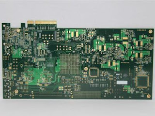
Blind & Buried VIA Hole PCB

Image
Custom blind and buried vias fabrication  from professional and experienced pcb board supplier at low cost. B lind and B uried V ia First of all, we start with traditional multi-layer boards. The structure of a standard multi-layer circuit board is a process including an inner layer line and an outer layer line, followed by drilling, and metallization in the hole to achieve the internal connection function of each layer line. However, due to the increase in line density, the way parts are packaged is constantly updated. In order to allow for a wider board area, more high-performance parts can be placed. In addition to the thinner line width, the aperture is also reduced from 1 mm in the DIP jack to 0.6 mm in SMD, and further reduced to 0.4 mm or less. However, the surface area is still occupied, so that there are buried holes and blind holes. The Buried Holes and Blind Holes are Defined as Follows Blind Vias: A blind via is a type of via that connects the inner trace of the PC

Edge Plating/Half-hole PCB

Image
Half hole pcb The walls of the PTH holes on the PCB are plated with Half-hole formed by smooth and complete metal forming.The Half hole pcb edge plating process   of the board is already a mature process in PCBSKY PCB manufacturing processing. How to control the quality of the product after forming the Half-hole on the edge of the board. For example, the copper spurs of the hole wall and the residue have always been a problem in the processing. This type of board has a row of half hole in the PCB, which is characterized by a relatively small aperture, mostly used on the carrier board, as a daughter board of the motherboard, through the half-hole and the motherboard and components The feet are welded together. Therefore, if there are copper thorns remaining in these half-hole, the soldering of the plug-in manufacturers will result in inaccurate solder joints and weak soldering, which will cause a bridge short circuit between the two pins. Half hole pcb has a minimum p

Flexible PCB

Image
Custom flexible pcb board from PCBSKY,   flex pcb china   manufacturer in china shenzhen, a TRUE PCB MANUFACTURER. Because of the advantages (for example, cost, space, and weight savings) that flexible and Rigid-Flex-circuit boards have for some projects, they are used ever more frequently. PCBSKY can produce your flexible circuit boards with the highest quality, either as prototype or as series with 1-10 layers. F lexible pcb prototype The standard surface used is chemical gold (ENIG), the contours are formed according to requirements, preferably using laser cutting, or also with mechanical milling. You should discuss the selected materials and design for the construction and layout of flexible circuit boards with us in the planning phase; we can assist you to work out the optimum solution! Exploring the Many Advantages of Flex Circuit Boards Reduced Space and Weight: Most of the advantages associated with flexible PCBs come from their low volume and weight. In fact, usin

Gold Fingers PCB

Image
Among the large-scale use of PCI and optical modules and cable sockets, the gold fingers PCB has been divided into: long and short gold fingers, broken gold fingers, split gold fingers, gold finger plates in the process of processing, need to pull gold-plated wire, conventional gold finger processing is relatively simple, the length of the gold finger PCB requires strict control of the gold finger lead and requires a second etching to complete. Broken gold finger PCB than length The difficulty of the gold finger is increased, and the dry film is required to be processed three times. The lead does not need to be left for 4 times to complete the production of the gold finger .90% of companies are unable to process the control of the golden finger. PCBSky processing plug gold fingers PCB and long and short gold fingers PCB, broken section Gold finger PCB, master the core manufacturing technology, single gold finger gold plating thickness up to 50U gold thick, industrial graphics card PCI

Hard Gold PCB

Image
Hard Gold PCB , immersion gold pcb, is to immerse the board in the plating tank and apply current to form a nickel-gold coating on the copper foil surface of the board. The electro-nickel gold is characterized by high hardness, wear resistance and oxidation resistance. Widely used in applications. Introduction to Hard Gold PCB Technology: 1. Purpose and role: gold as a precious metal, has good weldability, oxidation resistance, corrosion resistance, small contact resistance, good wear resistance of the alloy and so on; 2. At present, the electroplating gold of the circuit board is mainly a citrate gold bath, which is widely used for its simple maintenance and simple and convenient operation; 3. Water gold content is controlled at about 1 gram / liter, PH value of about 4.5, temperature of 35 degrees, specific gravity of about 14 waves, current density of about 1ASD; 4. The main added drugs are acid-adjusted salt and basic-adjusted salt for adjusting pH value, conduct