Posts

Showing posts from February, 2020

Via in Pad

Image
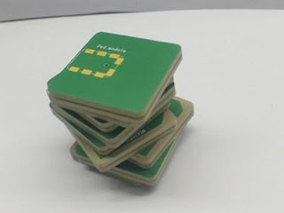
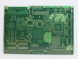
What is In Pad   Via   The holes drilled on the chip pads on the PCB can be referred to as VIA IN PAD. In the manufacturing process, after the via plating, the resin is filled and then the surface is plated and filled, and the via is not visible when the patch is applied. As we all know, via in pad technology, the PCB plugging process is a process that is produced by the higher requirements of the PCB manufacturing process and the surface mount technology. The via hole plugging  Effect has the Following Points • Prevents short-circuiting of tin from the via through the component surface during PCB over-wave soldering • Avoid flux remaining in the vias • Prevent the soldering of the solder balls from over-wave soldering, causing a short circuit • Prevent surface solder paste from flowing into the hole to cause solder joints, affecting placement The advantage of the resin plug hole relative to the solder resist plug hole is that the flatness of the pad of

Thick/Heavy Copper PCB

Image
Are you looking for heavy copper pcb manufacturers ? Thick Copper PCB Difinition and Thickness There is no exact definition of thick copper in the PCB industry. Generally, the copper thickness ≥ 2oz is defined as Heavy copper PCB. Heavy copper PCB is mainly used in high-current electronic products. High-current electronic products are generally high-power or high-voltage PCBs. They are mostly used in automotive electronics, communication equipment, aerospace, planar transformers, and secondary power modules. Our thickest copper PCB oz   can make 6 ounces. However, considering the side eclipse factor, 3 oz copper thickness  of more than 3 ounces should pay special attention to the line width of the inner layer. Inner 3 oz copper pcb : line width 6/7 mil outer 3 ounces: line width 8/12 mil Inner layer 4 oz copper pcb : line width line spacing 8/11 mil outer layer 3 ounces: line width line spacing 9/15 mil Inner 5 oz copper pcb: line width 10/16 mil outer 3 ounces

Rogers PCB

Image
What is rogers 4350 datasheet ? Rogers PCB , High Frequency PCB,RF PCB  (Enquiry pls send to Sales@pcbsky.com ) Supporting the military is something PCBSky is very proud of, and we were contracted to assemble a PCB for use in a military communications application. The RF PCB assembly used Rogers 4350 , Rogers 4003,RT5880  material, and the board required surface mount technology for the double-sided assembly that featured 250 placements. Board specs included 3 layers, standard vias, and 1 panelization. Final measurements came to 8 x 5.75 in. We performed final testing using automated optical inspections and x-ray inspection before delivering product to the customer. Serving industries from consumer to military, we continuously strive to build Rogers PCB products that exceed your expectations, to develop long-term customer relationships, and to become your best possible manufacturing partner. Rogers PCB Material in Stock Normally: Rogers 4350B rogers 4003c

PTFE Teflon PCB

Image
PTFE Teflon PCB has excellent comprehensive performance: high temperature resistance (-192°C-260°C), corrosion resistance (strong acid, strong alkali, aqua regia, etc.), weather resistance, high insulation, high lubrication, no adhesion, Non-toxic and other excellent characteristics. At present, various types of PTFE products have played a pivotal role in the national economy such as chemical, machinery, electronics, electrical appliances, military, aerospace, environmental protection and bridges. PTFE Teflon PCB Application The PTFE Teflon PCB is suitable for use in electrical insulation materials and linings, supporting sliders, rail seals and lubricating materials for electrical insulating materials and contact corrosive media. It is used in light industry in rich cabinet furniture. It is widely used in chemical, pharmaceutical, dye container, storage tank, reaction tower kettle, anti-corrosion lining material for large pipelines; heavy industry such as aviati

Multi-layer Flexible PCB

Image
multi layer flexible pcb  uses single-sided FCCL and adhesive as the base materials, the similar technology of Double-sided FPC with the method of single side, double access; through several times of lamination. It can be designed to the structure of partly delaminated in order to enhance the flexibility. The most typical difference between a multi-layer FPC and a single-layer FPC is the addition of a via structure to join the layers of copper foil. Flexible printed circuit boards are an important class of PCBs. Its characteristics are specifically: (1) FPC is small in size and light in weight. (2) FPC can be moved, bent, and twisted. (3) FPC has excellent electrical properties, dielectric properties and heat resistance. (4) FPC has higher assembly reliability and assembly operability. (5) FPC can be installed in three connections. (6) FPC is good for heat diffusion. (7) Low cost. (8) Continuity of processing. M ultilayer flex circuits   are widely

Metal Core PCB

Image
Custom low cost metal core pcb from professional pcb manufacturer china shenzhen, PCBSKY provides best service metal core pcb prototype. MCPCB, Metal Core PCB, thermal PCB -  whichever name you prefer, they are all boards which use a base metal material as the heat spreader portion of the circuit board. Base metals in the MCPCB fabrication   are used as an alternative to FR4 or CEM3 boards for the ability to dissipate heat away from critical board components and to less crucial areas such as the metal heatsink backing or metallic core. Metal Core PCB Materials and Thickness The metal core of the thermal PCB can be aluminum (aluminum core PCB), copper (copper core PCB or a heavy copper PCB) or a mixture of special alloys. The most common is an aluminum core PCB. The thickness of metal cores in PCB base plates is typically 30 mil - 125 mil, but thicker and thinner plates are possible. MCPCB copper foil thickness can be 1 - 10 oz. Advantages of MCPCB MCPCBs c

Impedance Control PCB

Image
W hat is impedance control in pcb ? High Speed PCB with Impedance Control Impedance Control PCB  refers to the PCB that needs impedance control. Impedance control refers to the “resistance” generated by a certain circuit layer under its high-frequency signal to its reference layer, and its signal must be controlled within the rated range to ensure that the signal is not distorted during transmission. Impedance control is to make each part of the system have the same impedance value, that is, impedance matching. Most high speed circuit boards currently have impedance control requirements. Therefore, it has also been said that a PCB board that does not have impedance control cannot be called a high speed PCB. Definition & Types of Characteristic Impedance At a certain frequency, the resistance of a high frequency signal or electromagnetic wave in the propagation of a signal line of an electronic device relative to a certain reference layer is called a characte

High Tg PCB

Image
What is High Tg PCB When the temperature rises to a certain area, the substrate will change from "glass state" to "rubber state", and the temperature at this time is called the glass transition temperature (Tg) of the plate. That is, Tg is the highest temperature (°C) at which the substrate remains rigid. That is to say, the ordinary PCB substrate material not only softens, deforms, melts, etc. at high temperatures, but also exhibits a sharp drop in mechanical and electrical properties. The general Tg of the PCB is 130 degrees or more, the high Tg is generally greater than tg170 pcb , and the medium Tg is greater than about tg 150 degrees . A PCB board with a typical Tg ≥ 170 ° C is called a high Tg board. The higher the pcb tg  value, the more resistant the sheet is to deformation and the better its dimensional stability. The substrate material of IPC-4101B (2006) standard epoxy/E type fiberglass cloth is divided into three grades according to

High Frequency PCB

Image
Custom high frequency pcb  from professional pcb manufacturer china shenzhen with factory price in low cost. The high frequency of electronic equipment is a development trend, especially in the development of wireless networks and satellite communications, the high-speed and high-frequency information products, and the standardization of voice, video and data for wireless transmissions with large capacity and fast communication products. A new generation of products that require high-frequency substrates. High Frequency PCB, HF PCB Types as below: ROGERS PCB PTFE TEFLON PCB FR4+HIGH FREQUENCY PCB High Frequency PCB Features 1, the impedance control requirements are more stringent, the relative line width control is very strict, the general tolerance is about 2%. 2. Due to the special plate, the adhesion of PTH to copper is not high. It is usually necessary to roughen the via and surface by means of plasma processing equipment to increase the adhesion of PTH

HDI PCB

Image
Are you looking for a reliable hdi pcb factory ? HDI PCBs, one of the fastest growing technologies in PCBs, are now available at PCBSky. HDI PCBs contain blind and/or buried vias and often contain microvias of .006 or less in diameter. They have a higher circuitry density than traditional circuit boards. There are 6 different types of HDI PCBs, through vias from surface to surface, with buried vias and through vias, two or more HDI layer with through vias, passive substrate with no electrical connection, coreless construction using layer pairs and alternate constructions of coreless constructions using layer pairs. HDI any-layer printed circuit boards are the next technological enhancement of HDI microvia printed circuit boards: all the electrical connections between the individual layers consist of laser-drilled microvias. The main advantage of this technology is that all the layers can be freely interconnected. To produce these circuit boards, PCBSky uses laser-drilled