Posts

Showing posts from October, 2019

Via in Pad

Image
What is Via In Pad The holes drilled on the chip pads on the PCB can be referred to as VIA IN PAD. In the manufacturing process, after the via plating, the resin is filled and then the surface is plated and filled, and the via is not visible when the patch is applied. As we all know, via in pad technology, the PCB plugging process is a process that is produced by the higher requirements of the PCB manufacturing process and the surface mount technology. The VIA Plugging In PCB  Effect has the Following Points • Prevents short-circuiting of tin from the via through the component surface during PCB over-wave soldering • Avoid flux remaining in the vias • Prevent the soldering of the solder balls from over-wave soldering, causing a short circuit • Prevent surface solder paste from flowing into the hole to cause solder joints, affecting placement The advantage of the resin plug hole relative to the solder resist plug hole is that the flatness of the pad of the resin p

Rogers PCB

Image
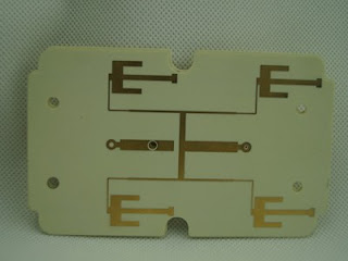
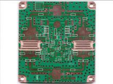
Rogers PCB , High Frequency PCB,RF PCB  (Enquiry pls send to Sales@pcbsky.com ) Supporting the military is something PCBSky is very proud of, and we were contracted to assemble a PCB for use in a military communications application. The RF PCB assembly used Rogers 4350, Rogers 4003,RT5880  material, and the board required surface mount technology for the double-sided assembly that featured 250 placements. Board specs included 3 layers, standard vias, and 1 panelization. Final measurements came to 8 x 5.75 in. We performed final testing using automated optical inspections and x-ray inspection before delivering product to the customer. Serving industries from consumer to military, we continuously strive to build Rogers PCB products that exceed your expectations, to develop long-term customer relationships, and to become your best possible manufacturing partner. Rogers PCB Material in Stock Normally: Rogers 4350B Rogers 4003C Rogers 3003 RT5880 RT5870 Right now,

PTFE Teflon PCB

Image
PTFE Teflon PCB has excellent comprehensive performance: high temperature resistance (-192°C-260°C), corrosion resistance (strong acid, strong alkali, aqua regia, etc.), weather resistance, high insulation, high lubrication, no adhesion, Non-toxic and other excellent characteristics. At present, various types of PTFE products have played a pivotal role in the national economy such as chemical, machinery, electronics, electrical appliances, military, aerospace, environmental protection and bridges. PTFE Teflon PCB Application The PTFE Teflon PCB board   is suitable for use in electrical insulation materials and linings, supporting sliders, rail seals and lubricating materials for electrical insulating materials and contact corrosive media. It is used in light industry in rich cabinet furniture. It is widely used in chemical, pharmaceutical, dye container, storage tank, reaction tower kettle, anti-corrosion lining material for large pipelines; heavy industry such as aviation

Metal Core PCB

Image
Custom low cost metal core pcb from professional pcb manufacturer china shenzhen, PCBSKY provides best service metal core pcb prototype   . MCPCB, Metal Core PCB, thermal PCB , mcpcb fabrication  -  whichever name you prefer, they are all boards which use a base metal material as the heat spreader portion of the circuit board. Base metals in the MCPCB board   are used as an alternative to FR4 or CEM3 boards for the ability to dissipate heat away from critical board components and to less crucial areas such as the metal heatsink backing or metallic core. Metal Core PCB Materials and Thickness The metal core of the thermal PCB can be aluminum (aluminum core PCB), copper (copper core PCB or a heavy copper PCB) or a mixture of special alloys. The most common is an aluminum core PCB. The thickness of metal cores in PCB base plates is typically 30 mil - 125 mil, but thicker and thinner plates are possible. MCPCB copper foil thickness can be 1 - 10 oz. Advantages of MCPCB

Education

Image
PCB Education Students are our future engineers who will re-shape the world surrounding us. Some of the most creative and audacious electronic research comes from our students in universities or even high schools. Therefore PCBSky.com feels proud to sponsor teachers and students for their PCB needs. The biggest challenge of modern electronics is that the components are so miniaturized that students can no longer use universal boards and the parts can no longer be reliably hand soldered. By streamlining manufacturing processes, PCBSky.com is capable to fabricate your PCBs in as short as 12 hours, and offers PCB assembly under one roof as a consecutive service. Our strong network of parts suppliers makes the sourcing quick, reliable and cost-effective.