Posts

Showing posts from September, 2019

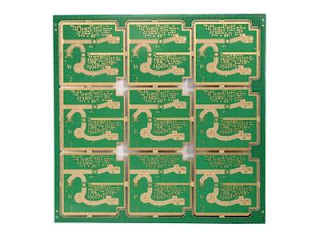
Role of auxiliary components in hard gold plating PCB plating solution

Electroplating can be divided into hard gold and soft gold. Hard gold electroplating is an alloy, so its hardness is relatively hard. It is suitable for use in places requiring force and friction. It is generally used as the edge contact point of PCB (commonly known as golden finger). Soft gold, On the other hand, is commonly used to connect aluminum wires On the COB (Chip On Board) or On the touch surface of mobile phone keys, and more recently, it is widely used On both sides of BGA boards. The distinction of hard gold and soft gold, it is the component of this layer of gold that goes up finally plating, when gold-plating can choose electroplate pure gold or alloy, because the hardness of pure gold is softer, so also call "soft gold". Function of auxiliary components in PCB plating hard gold plating solution : Boric acid ACTS: as a buffer, which can maintain a relatively balanced PH value of hard gold-plated PCB plating solution with a concentration of 35~55g/l;

Thick/Heavy Copper PCB

Image
Thick Copper PCB Difinition and Thickness There is no exact definition of thick copper in the PCB industry. Generally, the copper thickness ≥ 2oz is defined as Heavy copper PCB. Heavy copper PCB is mainly used in high-current electronic products. High-current electronic products are generally high-power or high-voltage PCBs. They are mostly used in automotive electronics, communication equipment, aerospace, planar transformers, and secondary power modules. Our thickest copper PCB can make 6 ounces. However, considering the side eclipse factor, copper thickness of more than 3 ounces should pay special attention to the line width of the inner layer. Inner 3 oz copper pcb: line width 6/7 mil outer 3 ounces: line width 8/12 mil Inner layer 4 oz copper pcb: line width line spacing 8/11 mil outer layer 3 ounces: line width line spacing 9/15 mil Inner 5 oz copper pcb: line width 10/16 mil outer 3 ounces: line width 11/16 mil Inner 6 oz copper pcb : line width line spacing 12/

PTFE Teflon PCB

Image
PTFE Teflon PCB has excellent comprehensive performance: high temperature resistance (-192°C-260°C), corrosion resistance (strong acid, strong alkali, aqua regia, etc.), weather resistance, high insulation, high lubrication, no adhesion, Non-toxic and other excellent characteristics. At present, various types of PTFE pcb board  have played a pivotal role in the national economy such as chemical, machinery, electronics, electrical appliances, military, aerospace, environmental protection and bridges. And we are a professional teflon pcb manufacturer .   PTFE Teflon PCB Application The PTFE Teflon PCB is suitable for use in electrical insulation materials and linings, supporting sliders, rail seals and lubricating materials for electrical insulating materials and contact corrosive media. It is used in light industry in rich cabinet furniture. It is widely used in chemical, pharmaceutical, dye container, storage tank, reaction tower kettle, anti-corrosion lining material for la

Metal Core PCB

Image
Custom low cost metal core pcb  from professional pcb manufacturer china shenzhen, PCBSKY provides best service metal core pcb prototype. MCPCB, Metal aluminium Core PCB , thermal PCB -  whichever name you prefer, they are all boards which use a base metal material as the heat spreader portion of the circuit board. Base metals in the MCPCB are used as an alternative to FR4 or CEM3 boards for the ability to dissipate heat away from critical board components and to less crucial areas such as the metal heatsink backing or metallic core. Metal Core PCB Fabrication Materials  and Thickness The metal core of the thermal PCB can be aluminum (aluminum core PCB), copper (copper core PCB or a heavy copper PCB) or a mixture of special alloys. The most common is an aluminum core PCB. The thickness of metal cores in PCB base plates is typically 30 mil - 125 mil, but thicker and thinner plates are possible. MCPCB copper foil thickness can be 1 - 10 oz. Advantages of MCPCB fabricat

High Frequency PCB

Image
Custom high frequency pcb from professional pcb manufacturer china shenzhen with factory price in low cost. The high frequency of electronic equipment is a development trend, especially in the development of wireless networks and satellite communications, the high-speed and high-frequency information products, and the standardization of voice, video and data for wireless transmissions with large capacity and fast communication products. A new generation of products that require high-frequency substrates. High Frequency PCB, HF PCB Types as below: ROGERS PCB PTFE TEFLON PCB FR4+HIGH FREQUENCY PCB High Frequency PCB Features 1, the impedance control requirements are more stringent, the relative line width control is very strict, the general tolerance is about 2%. 2. Due to the special plate, the adhesion of PTH to copper is not high. It is usually necessary to roughen the via and surface by means of plasma processing equipment to increase the adhesion of PTH hole coppe

HDI PCB

Image
HDI PCBs, one of the fastest growing technologies in PCBs, are now available at PCBSky. HDI PCBs contain blind and/or buried vias and often contain microvias of .006 or less in diameter. They have a higher circuitry density than traditional circuit boards. There are 6 different types of HDI PCBs, through vias from surface to surface, with buried vias and through vias, two or more HDI layer with through vias, passive substrate with no electrical connection, coreless construction using layer pairs and alternate constructions of coreless constructions using layer pairs. HDI any-layer printed circuit boards are the next technological enhancement of HDI microvia printed circuit boards: all the electrical connections between the individual layers consist of laser-drilled microvias. The main advantage of this technology is that all the layers can be freely interconnected. To produce these circuit boards, PCBSky uses laser-drilled microvias electroplated with copper. Special Tec

Hard Gold PCB

Image
Hard Gold PCB, immersion gold pcb, is to immerse the board in the plating tank and apply current to form a nickel-gold coating on the copper foil surface of the board. The electro-nickel gold is characterized by high hardness, wear resistance and oxidation resistance. Widely used in applications. Introduction to Hard Gold PCB Technology: 1. Purpose and role: gold as a precious metal, has good weldability, oxidation resistance, corrosion resistance, small contact resistance, good wear resistance of the alloy and so on; 2. At present, the electroplating gold of the circuit board is mainly a citrate gold bath, which is widely used for its simple maintenance and simple and convenient operation; 3. Water gold content is controlled at about 1 gram / liter, PH value of about 4.5, temperature of 35 degrees, specific gravity of about 14 waves, current density of about 1ASD; 4. The main added drugs are acid-adjusted salt and basic-adjusted salt for adjusting pH value, conducti