Posts

Gold Fingers PCB

Image
Among the large-scale use of PCI and optical modules and cable sockets, the gold fingers PCB has been divided into: long and short gold fingers, broken gold fingers, split gold fingers, gold finger plates in the process of processing, need to pull gold-plated wire, conventional gold finger processing is relatively simple, the length of the circuit board fingers  require strict control of the gold finger lead and requires a second etching to complete. Broken gold finger PCB than length The difficulty of the gold finger is increased, and the dry film is required to be processed three times. The lead does not need to be left for 4 times to complete the production of the gold finger .90% of companies are unable to process the control of the golden finger. PCBSky processing plug gold fingers PCB and long and short gold fingers PCB, broken section Gold finger PCB, master the core manufacturing technology, single gold finger plating  thickness up to 50U gold thick, industrial graphi...

Edge Plating/Half-hole PCB

Image
Half hole pcb The walls of the PTH holes on the PCB are plated with Half-hole formed by smooth and complete metal forming.The Half hole process on the edge of the board is already a mature process in PCBSKY PCB manufacturing processing. How to control the quality of the product after forming the Half-hole on the edge of the board. For example, the copper spurs of the hole wall and the residue have always been a problem in the processing. This type of board has a row of half hole in the PCB, which is characterized by a relatively small aperture, mostly used on the carrier board, as a daughter board of the motherboard, through the half-hole and the motherboard and components The feet are welded together. Therefore, if there are copper thorns remaining in these half-hole, the soldering of the plug-in manufacturers will result in inaccurate solder joints and weak soldering, which will cause a bridge short circuit between the two pins. Half hole pcb has a minimum processi...

Double Sided Flexible PCB

Image
After the double-sided PI board copper-clad board material is used in the double-sided circuit, a protective film is added on both sides to form a circuit board having a double-layer conductor. The Structure of the Double-layer FPC When the circuit of the circuit is too complicated, the single-layer fpc cannot be wired or copper foil is needed for ground shielding, it is necessary to select a double-layer fpc or even a multi-layer fpc. The most typical difference between a multi-layer fpc and a single-layer fpc is the addition of a via structure to join the layers of copper foil. The first processing technique of general substrate + transparent rubber + copper foil is to make via holes. First drill holes in the substrate and copper foil, after plating, a certain thickness of copper is plated, and the via holes are completed. The subsequent production process is almost the same as that of a single layer. Double-panel structure: Both sides of the double-sided panel have pads, whic...

Blind & Buried VIA PCB

Image
Custom blind and buried vias fabrication  from professional and experienced pcb board supplier at low cost. First of all, we start with traditional multi-layer boards. The structure of a standard multi-layer circuit board is a process including an inner layer line and an outer layer line, followed by drilling, and metallization in the hole to achieve the internal connection function of each layer line. However, due to the increase in line density, the way parts are packaged is constantly updated. In order to allow for a wider board area, more high-performance parts can be placed. In addition to the thinner line width, the aperture is also reduced from 1 mm in the DIP jack to 0.6 mm in SMD, and further reduced to 0.4 mm or less. However, the surface area is still occupied, so that there are buried holes and blind holes. The Buried Holes and Blind Holes are Defined as Follows Blind Vias: A blind via is a type of via that connects the inner trace of the PCB to the trace of ...

PCB Assembly

Image
PCBSKY is a national enterprise focusing on PCB and PCBA manufacturing for 8 years. The company has a strong engineering team and a professional electronic component procurement team to serve many domestic and foreign automotive electronics, medical electronics, power communication, industrial automation and smart home. Customers in various industries, is a one-stop manufacturing service provider integrating PCB manufacturing, electronic component acquisition, SMT chip processing and test assembly. Our company provides PCBA electronic manufacturing solutions for customers in developed countries and regions such as the United States, Canada, Germany, France, Hong Kong, etc., and has won good reputation, including PCB board manufacturing and SMT chip processing and other core businesses. Self-developed SMT patch online quotation ordering system, the quotation is accurate and hidden, the procurement is efficient and convenient; the production of ERP system in the docking factory,...

LED

Image
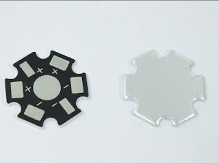
We are professional LED PCB manufacturer . We offer all kinds of LED PCB Product  and our LED PCB price  is competitive.  For High-Power LED of the Aluminum Base PCB, copper base PCB, ceramic base PCB, for low-power LED of the FR4 PCB, High-Temperature PCB. As the Aluminum Base PCB of good thermal performance, High-Power LED products most commonly used Aluminum Base PCB.   We can give different Solder mask options for your Led PCB ,We do lots of R&D on Led PCB solder mask  Lumens to give your Led lights better brightness . The Applications of LED PCB Circuit Board The Led benefits  make LED printed circuit boards  very desirable for a number of applications and industries. Some of the more prominent applications of Aluminum LED PCB Circuit Board include:Telecom LED PCB,Automotive LED PCB,Computer Led PCB,Medical LED PCB,Led PCB Products :  Led Tube , Outdoor LED advertising screen, LED Lamp, Waterpr...

Education

Image
Students are our future engineers who will re-shape the world surrounding us. Some of the most creative and audacious electronic research comes from our students in universities or even high schools.   PCB education  is important nowadays.  Therefore PCBSky.com feels proud to sponsor teachers and students for their PCB needs. The biggest challenge of modern electronics is that the components are so miniaturized that students can no longer use universal boards and the parts can no longer be reliably hand soldered. By streamlining manufacturing processes, PCBSky.com is capable to fabricate your PCBs in as short as 12 hours, and offers PCB assembly under one roof as a consecutive service. Our strong network of parts suppliers makes the sourcing quick, reliable and cost-effective.

What is pcb used for?

With the development of science and technology, the application of PCB is more and more extensive. PCB is divided into single-sided PCB, double-sided PCB and multi-layer PCB. Common multi-layer boards are generally 4-layer PCB or 6-layer PCB, complex multi-layer board. It can be used in dozens of layers and is widely used in consumer electronics, computers, communication tools, medical equipment and other fields. In terms of application industry distribution, consumer electronics accounted for the highest proportion, up to 39%; followed by computer accounted for 22%; communication accounted for 14%; industrial control, medical instruments accounted for 14%; automotive electronics accounted for 6%; Aerospace accounts for 5% of the total, and the requirements for PCB precision in aerospace and medical instruments are very high. Although China's current PCB industry scale is the world's first, but from the overall technical level, it still lags behind the world's advanced leve...

Computers&SSD

Image
The PCB on the computer consists of a motherboard, a hard disk, a memory module, a graphics card, and the like. The plane of the computer motherboard is a PCB (printed circuit board), generally four or six layers. Relatively speaking, in order to save costs, the low-end motherboards are mostly four-layer boards: the main signal layer, the ground layer, the power layer, and the sub-signal layer, while the six-layer board adds the auxiliary power layer and the middle signal layer. Therefore, the six-layer PCB The motherboard is more resistant to electromagnetic interference and the motherboard is more stable. You won't find electronics PCBs today only in computers - although laptops, smartphones, desktops and tablets certainly can't function without quality printed circuit boards, and printed circuit boards for computers make up a large part of the industry. Instead, you'll find machines containing printed circuit boards almost everywhere you look. Your television, wireless ...

Warmly celebrate our company's national high-tech enterprise certification

Image
After more than a year of hard work, our company finally passed the national high-tech enterprise certification.

What are the Factors that Affect the Price of PCB Processing

PCB processing belongs to the OEM customer's OEM products. Different customers order different products, and there are few shared products. On the other hand, some customers may specify the use of a manufacturer's substrate for quality considerations. Ink and so on, in order to achieve its quality and cost control requirements, so PCB processing prices are changeable. What are the factors that affect the price of PCB processing? Basically consists of the following factors: First, the materials used in the PCB are different. Taking ordinary double-panel as an example, the sheets generally have FR-4, CEM-3, etc., the thickness ranges from 0.6mm to 3.0mm, and the thickness of copper varies from 1oz to 3oz. The price varies greatly from specification to specification; In terms of ink, there is also a price difference between ordinary thermosetting ink and photosensitive green ink, so the difference in materials causes price diversity. Second, the PCB uses different production proc...

Role of auxiliary components in hard gold plating PCB plating solution

Image
Electroplating can be divided into hard gold and soft gold. Hard gold electroplating is an alloy, so its hardness is relatively hard. It is suitable for use in places requiring force and friction. It is generally used as the edge contact point of PCB (commonly known as golden finger). Soft gold, On the other hand, is commonly used to connect aluminum wires On the COB (Chip On Board) or On the touch surface of mobile phone keys, and more recently, it is widely used On both sides of BGA boards. The distinction of hard gold and soft gold, it is the component of this layer of gold that goes up finally plating, when gold-plating can choose electroplate pure gold or alloy, because the hardness of pure gold is softer, so also call "soft gold". Function of auxiliary components in   hard gold plating PCB   plating solution: Boric acid ACTS: as a buffer, which can maintain a relatively balanced PH value of hard gold-plated PCB plating solution with a concentration of 35~55g/l; N...

What Information does the PCB Prototype Need to Give the Manufacturer

Recently, many customers asked the PCB Prototype what information to provide, and today I will give you a comprehensive answer. PCB Prototype is an early step in mass production. Only when proofing is accurate, can it be put into mass production. Therefore, it is especially important to provide accurate proofing files. So, do you know what documents you need to provide? And what issues should I pay attention to in the documentation provided? First, you need to provide a PCB or GERBER file, the document should include the plate-making instructions - including the specific number of board layers, materials, pad process, ink color, etc., here are some specific parameters to explain. Material: To explain what kind of PCB material is needed, the most common one is FR4. The main material is epoxy resin stripping fiber board. Slab: Describe the number of layers in the PCB. (The PCB production layer is different, the price will be different, and the PCB Prototype process is much the same) Sold...

This PCB Manufacturer is Different

We often hear that PCBs are everywhere in the Shenzhen area of China. In our eyes, the PCB factory is a particularly cheap factory, but this board manufacturer is different. What is the truth? This board processing plant has a strict quality control system: 1 product meets IPC-II or IPC-III standards 2 use SPC management chart for quality process control 3 Implement PDCA cycle process to continuously improve product performance 4 Established a complete quality assurance inspection system, the entire process is equipped with professional quality assurance personnel In the circuit board industry, there are often customer complaints that the delivery time is not on time, and the pcb is not good. Is this the circuit board factory supplier has no choice? Or is the operator not worried? PCBSKY has rich experience in PCB production. As a PCB manufacturer, we have excellent process R&D team, stable production team, strict quality assurance team, excellent quality, accurate delivery and goo...

10 PCB Puzzle Secrets

1. The outer frame (clamping edge) of the  custom pcb fabrication  should adopt a closed-loop design to ensure that the PCB panel will not be deformed after being fixed on the fixture. 2. The width of the custom pcb fabrication is less than or equal to 260mm (SIEMENS line) or less than or equal to 300mm (FUJI line); if automatic dispensing is required, the product of the width and length of the PCB board is less than or equal to 125 mm × 180 mm. 3. Custom pcb fabrication shape should be as close to square as possible. It is recommended to use 2×2, 3×3 jigsaw, but do not spell into yin and yang boards. 4. The center distance between the small plates is controlled between 75mm and 145mm. 5. When setting the reference positioning point, usually leave a non-resistive soldering area 1.5mm larger than the positioning point. 6. There should be no large devices or protruding devices near the connection point between the outer frame of the panel and the inner small plate, small plate a...

PCB Circuit Board Customization

The general  custom pcb fabrication   design process is as follows: pre-preparation -> PCB structure design -> PCB layout -> wiring -> wiring optimization and silk screen -> network and DRC inspection and structural inspection -> plate making Preliminary preparation This includes preparing component libraries and schematics. PCB structure design According to the determined board size and various mechanical positioning, draw the PCB surface in the PCB design environment, and place the required connectors, buttons/switches, screw holes, assembly holes, etc. according to the positioning requirements. And fully consider and determine the wiring area and non-wiring area. The assembly drawing is printed after the layout is completed. The assembly drawing is used by the schematic designer to check the correctness of the device package and to confirm the signal correspondence between the board, the backplane and the connector. The wiring can be started after co...

Relevant introduction of aluminum printed circuit boards

Image
Aluminum printed circuit board (PCB)  is a kind of PCB: Aluminum printed circuit board (PCB) is a kind of metal base copper clad board with good heat dissipation function. Generally, a single panel is composed of three layers, which are circuit layer (copper foil), insulation layer and metal base. For high-end use there is also a design for double panels, the structure of the circuit layer, insulation layer, aluminum base, insulation layer, circuit layer. Very few applications for multilayer board, can be made of ordinary multilayer board and insulation layer, aluminum base laminated.  Single aluminum substrate: is only one layer of conductive graphics layer and insulation materials plus aluminum (substrate).  Double-sided line aluminum substrate: there are two layers of conductive graphics layer and insulation material plus aluminum (substrate) superimposed together.  Multilayer printed aluminum-based circuit board: a printed circuit board made by bonding th...

PCB Design Experience Summary: 10 Rules for Component Layout

1.  Custom pcb fabrication   follows the layout principle of “first big, then small, first difficult and easy”, that is, important unit circuits and core components should be prioritized. 2. The layout should refer to the principle block diagram, and arrange the main components according to the main signal flow direction of the board. 3. The arrangement of components should be easy to debug and repair, that is, there should be no space around the small components, and there should be enough space around the components to be debugged. 4. For the same structural circuit part, use the "symmetric" standard layout as much as possible. 5. Optimize the layout according to the standard of uniform distribution, balance of center of gravity, and beautiful layout. 6. The same type of instrumented components should be placed in one direction in the X or Y direction. The same type of polar discrete components must also strive to be consistent in the X or Y direction for ease of production...