Edge Plating/Half-hole PCB
Edge Plating/Half-hole PCB
Hard Gold PCB HARD GOLD PCBVia in Pad VIA IN PAD
PCB FABRICATION
Conventional PCB
Impedance Control PCB
Gold Fingers PCB
Hard Gold PCB
Thick / Heavy Copper PCB
Edge Plating/Half-hole PCB
High Tg PCB
Via in Pad
Metal Core PCB
High Frequency PCB
Flexible PCB
Blind & Buried VIA Hole PCB
SMT Assembly
Rigid-flex PCB
ARTICLE
Distinguish between Hard Gold and Soft Gold
What Is A Printed Circuit Board?
Design Type of Aluminum Printed Circuit Board
Manufacturing Structure of Multilayer Flexible Printed Board
CONATCT
Tel: +86-755-33583558 Ext 603
E-mail: service@pcbsky.com
Add: 407, Kanglan Fortune Center, Fuzhou Avenue, Fuyong Street, Baoan District, Shenzhen, Guangdong 518103, China
Half hole pcb
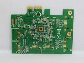
The walls of the PTH holes on the PCB are plated with Half-hole formed by smooth and complete metal forming.The Half hole process on the edge of the board is already a mature process in PCBSKY PCB manufacturing processing.
How to control product quality after forming half holes on the edge of the circuit board? For example, copper debris and residues on the hole walls have always been a problem in PCB edge plating process.
This type of board has a row of half hole in the PCB, which is characterized by a relatively small aperture, mostly used on the carrier board, as a daughter board of the motherboard, through the half-hole and the motherboard and components The feet are welded together.
Therefore, if there are copper thorns remaining in these half-hole, the soldering of the plug-in manufacturers will result in inaccurate solder joints and weak soldering, which will cause a bridge short circuit between the two pins.
Half hole pcb has a minimum processing capacity of 0.4 mm for the sample and a minimum of 0.5 mm for the batch.
Edge Plating does not have a set definition per IPC. However, the industry generally accepts this as being copper plating that continues from the top and bottom surfaces and along one or more perimeter edges. The process of Edge Plating PCB can be used for a variety of purposes, including, but not limited to edge soldering, edge connections, and to increase current carrying capacity. Burrs Often edge plating, especially on castellations, can result in burrs from the final machining process.
We apply a modified, proprietary process flow that results in the burrs being polished down to the edge of the feature. Copper Peeling Plating over a large substrate surface can lead to the plated copper peeling due to a lack of adhesion strength. We address this by first roughening the surface through a combination of chemical and other proprietary means. We then use direct metallization, which has a higher copper bond strength, to prepare the surface for plating.
Welcome to custom Edge Plating PCB / Half Hole PCB directly from PCB Factory at low cost.
CUSTOM PCB CHINA FABRICATION
PCBSKY is a professional PCB/FPC manufacturer in China, providing full PCB fabrication services in certified quality standards. We specialize in quick turn PCB & prototypes.

Comments
Post a Comment