How pcb is manufactured?
The manufacturing of a Printed Circuit Board (PCB) is a complex process that involves several steps. Here is an overview of how PCBs are typically manufactured:
1. Design and Layout: The PCB manufacturing process begins with the design and layout of the PCB. Designers use PCB design software to create a schematic diagram of the circuit and then lay out the components and traces on the PCB to ensure proper connectivity.
2. Gerber File Generation: Once the design is complete, the designer generates Gerber files. These files contain detailed information about the PCB's layers, component placements, and traces. Gerber files are essential for the fabrication process.
3. Material Selection: The next step involves selecting the materials for the PCB. The most common material is FR-4, a type of fiberglass-reinforced epoxy laminate. The choice of material depends on factors like the PCB's intended application and required electrical properties.
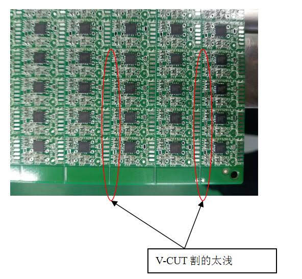
4. Panelization: Multiple PCBs are often fabricated together on a single larger panel. This process, known as panelization, helps optimize production efficiency.
5.Printed Circuit Board Etching:
- Subtractive Process: A layer of copper foil is laminated onto the substrate material. A chemical resist is applied to protect the copper that will become the traces. The board is then exposed to an etching solution, which removes the unwanted copper, leaving behind the desired traces.
6. Drilling: Holes are drilled through the PCB to create vias and to allow for component placement and interconnection between different layers. Computer Numerical Control (CNC) machines are commonly used for precise drilling.
7. Through-Hole Plating: After drilling, the PCB may undergo a through-hole plating process, where copper is plated onto the walls of the drilled holes to ensure electrical conductivity between layers.
8. Solder Mask Application: A solder mask layer is applied over the copper traces to insulate them and prevent unintentional solder bridges during assembly. The solder mask is typically green, but it can be other colors as well.
9. Silkscreen Printing: A silkscreen layer is applied to the PCB's surface to add component labels, reference designators, and other markings. This helps with component placement and soldering during assembly.
10. Surface Finish: The PCB's surface finish is applied to protect the exposed copper and improve solderability. Common surface finishes include HASL (Hot Air Solder Leveling), ENIG (Electroless Nickel Immersion Gold), and OSP (Organic Solderability Preservatives).
11. Testing: The manufactured PCBs undergo various testing procedures, including electrical testing to check for continuity and potential defects. Automated optical inspection (AOI) and X-ray inspection may also be used to detect manufacturing defects.
12. Routing and Separation: After testing, the panelized PCBs are separated into individual boards using a routing or depanelization process.
13. Final Inspection and Packaging: Each PCB is visually inspected for quality, and any necessary touch-up work is performed. The finished PCBs are then packaged and prepared for shipment to customers or assembly facilities.
Once the PCBs are manufactured, they can be populated with electronic components through a separate process called PCB assembly or soldering, where components are attached to the board and soldered in place to create a functional electronic device.
PCBSky is a professional PCB & Flex PCB manufacturer in China, providing full PCB fabrication and assembly services in certified quality standards. We specialize in quick turn PCB & prototypes.

Comments
Post a Comment